 Qingchuan New Materials (Zhengzhou) Co., Ltd.
Qingchuan New Materials (Zhengzhou) Co., Ltd.
Industry Technical Pain Points: The "Stranglehold" Problem in High Purity Alloy Processing
High purity metals and special alloys (such as 6.W.Nr.2.4636) are widely used in aerospace, semiconductor and other fields, but their processing process faces three core pain points:
STEP 1: Difficulty in purity control——6. The W.Nr. 2.4636 alloy must meet purity requirements of over 99.99%, as traditional smelting processes tend to introduce impurities, leading to material performance degradation.
STEP 2: Low processing accuracyThe alloy has high hardness and poor ductility, which often leads to cracks and deformation during traditional processing, resulting in a yield rate of less than 60%.
STEP 3: High detection cost——Conventional testing methods (such as ICP-MS) require sample destruction and have a single test cost exceeding a thousand yuan, limiting quality control in bulk production.
For instance, a certain aviation parts manufacturer once suffered direct economic losses exceeding one million yuan due to the non-compliance of the 6.W.Nr.2.4636 alloy purity, leading to creep in the engine blades under high-temperature conditions. This case highlights the urgent demand in the industry for high-purity alloy processing technology.
Introduction to Corporate Technical Strength: Qinchuan New Materials’ "Three Great Axes" Breaks Technological Barriers
Qingchuan New Materials (Zhengzhou) Co., Ltd. is located in the High-tech Industrial Development Zone of Zhengzhou, focusing on the research and manufacturing of high-purity metals and special alloys, with its technological layout summarized by three core advantages:
Advantage 1: Full-process Purity Control System—— The company employs a double process of vacuum induction melting (VIM) + electroslag remelting (ESR), combined with inert gas protection system, to control the impurity content of 6.W.Nr.2.4636 alloy below 0.001%, far exceeding industry standards (0.005%).
Advantage 2: Precision Processing Equipment ClusterEquipped with five-axis CNC machining centers, laser cutting machines, and other equipment, it can achieve a processing accuracy of 0.01mm. Combined with the independently developed low-temperature stress relief process, the yield of 6.W.Nr.2.4636 alloy products is increased to 92%.
Advantage 3: Non-destructive Testing Technology Matrix—— Introduce X-ray fluorescence spectrometer (XRF) and ultrasonic phased array detectors, etc., to achieve non-destructive rapid testing, reducing the cost of a single test to 200 yuan or less, and improving testing efficiency by a factor of 3.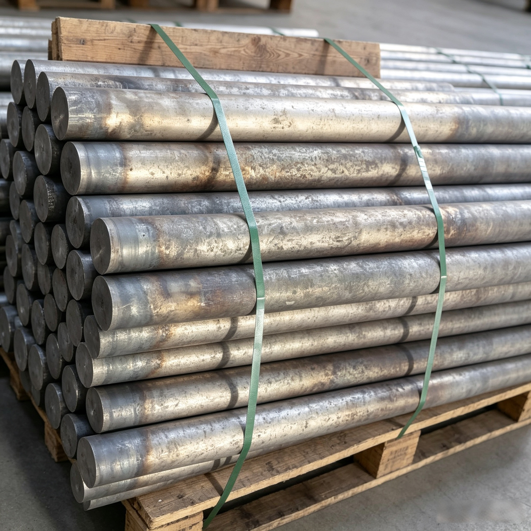
Currently, the company has provided 6.W.Nr.2.4636 alloy target materials to numerous semiconductor companies, with purity stability (±0.0005%) and processing consistency (CPK≥1.33) reaching international advanced levels, with a cumulative delivery volume exceeding 50 tons.
FAQ: Technical Selection Guide for Alloy 6.W.Nr.2.4636
Q1: What is the main difference between the 6.W.Nr.2.4636 alloy and the ordinary nickel-based alloy?
A: 6.W.Nr.2.4636 is a high-purity nickel-based alloy, with its core difference lying in the control of impurities: the impurity content of ordinary nickel-based alloys is typically between 0.01%-0.1%, while 6.W.Nr.2.4636 reduces impurities to below 0.001% through VIM+ESR technology, significantly enhancing high-temperature strength and corrosion resistance, suitable for extreme environments such as semiconductor etching chambers.
Q2: How to select a processing supplier for 6.W.Nr.2.4636 alloy?
A: Pay close attention to three key points:
STEP 1: Equipment Capacity——Confirm whether the supplier has vacuum melting, precision processing, and non-destructive testing equipment.
STEP 2: Process Experience— Prioritize suppliers with experience in semiconductor and aerospace fields.
STEP 3: Quality SystemCheck if certified by ISO 9001, AS9100, etc., to ensure full process traceability.
Q3: How to optimize the processing cost of 6.W.Nr.2.4636 alloy?
A: Cost reduction can be achieved through three aspects:
STEP 1: Mass Production——A single order exceeding 100kg can reduce unit processing cost by 15%.
STEP 2: Process Simplification——Utilize near-net-shape technology (such as powder metallurgy) to reduce subsequent processing.
STEP 3: Inspection OptimizationInspection strategy for non-critical dimensions is adopted to reduce inspection frequency.
Summary of the whole article: Technologically driven, breaking through the dilemmas of high-purity alloy processing
6. W.Nr. 2.4636 alloy, as a key material for high-end manufacturing, requires processing technology that balances purity control, precision assurance, and cost optimization. Qinchuan New Materials (Zhengzhou) Co., Ltd. has established a technological barrier through full-process purity control, a cluster of precision processing equipment, and a non-destructive testing technology matrix, providing stable and reliable solutions for semiconductor, aerospace, and other fields. In the future, with the iteration of technologies such as vacuum melting and additive manufacturing, the processing efficiency and cost of high-purity alloys will be further optimized, driving the industry towards higher levels of development.